Hello Robonesians, in the world of digital circuit design, whether for FPGAs or ASICs, there is one crucial stage before a design is realized into physical hardware: simulation. Simulation cannot be separated from the testbench, because the testbench is the “driving engine” that makes digital circuit design simulations possible.
For beginners, questions often arise:
- What is simulation?
- What is a testbench?
- Why can’t a design be directly downloaded to an FPGA?
- Why can a logically correct RTL still be wrong in hardware?
This article will explain the close relationship between simulation and testbench in a step-by-step and easy-to-understand manner, especially for those who are just starting to learn hardware description language (HDL), such as: VHDL, Verilog, and/or SystemVerilog.
1. What is Simulation in Digital Design?
1.1 Definition of Simulation
Simulation is the process of running a digital circuit model (RTL, register transfer level) in simulator software to observe the circuit’s behavior over time, without building physical hardware. Simulation is equivalent to a “virtual testbed” before the hardware is built.
By doing simulations, we can:
- View signal changes over time.
- Ensures that the digital circuit logic works according to specifications.
- Find bugs in HDL program code early, so they can be fixed quickly.
- Save costs and time.
1.2 What is Simulated?
What is simulated is:
- HDL program code is a digital circuit design or often called RTL (Register Transfer Level).
- Digital logic model.
- Behavior of sequential and/or combinational digital circuits.
Example:
- Counter.
- Adder (Half or Full).
- Register.
- FSM (Finite State Machine).
- UART.
- SPI.
- Memory controller.
- … and so forth
2. What is Testbench?
2.1 Definition of Testbench.
Testbench is a special HDL code used to:
- Provides stimulus (input) to the digital circuit design (RTL) built using HDL program code.
- Generates clock and reset.
- Observing the design output.
- Check whether the digital circuit output is correct or not.
2.2 Testbench Not Synthesized by Compiler.
Testbenches are not part of the digital circuit hardware design, so they are not synthesized by the compiler.
2.3 Why Can’t RTL Designs Be Simulated Alone?
Because digital circuit designs (RTL designs) created with HDL programming languages do not have natural input sources.
If you have any questions:
- Where does the clock come from?
- When is the reset active?
- Who provides input values?
- So the answer is: Testbench.
Without testbench:
- There is no clock, so the sequential circuit does not run.
- There is no input, so the output never changes.
- The simulator doesn’t know what to test.
So it can be analogized, if the RTL design is a “machine”, then the testbench is the “machine operator and testing tool”.
3. Relationship between Simulation and Testbench
3.1 Fundamental Relationships
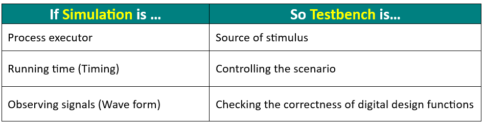
Simulation is a process, while a testbench is the controller of that process. Therefore, simulation and testbench are inseparable:
Table 1. Relationship between simulation and testbench
3.2 Illustration of Simulation and Testbench Concept
Imagine a washing machine:
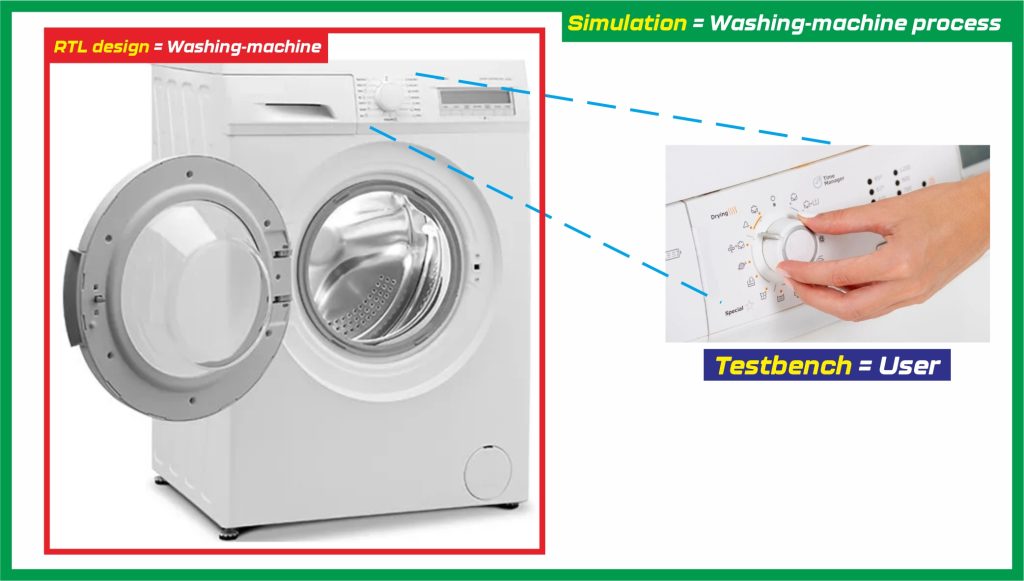
Figure 1. Simulation and testbench concept
If the ” RTL design ” is a washing machine, then the ” testbench ” is the person operating the washing machine (the user). Meanwhile, the ” simulation ” is the actual working process of the washing machine. Without a person (the user) adjusting the operating buttons on the washing machine, the washing machine would never operate.
4. Simulation Flow with Testbench
The following are the stages of simulation using a testbench:
- Create digital circuit design program code (VHDL/Verilog/SystemVerilog).
- Create testbench program code.
- RTL is instantiated in the testbench (DUT).
- The testbench provides clock, reset, and input.
- Time running simulator.
- Output is observed or checked automatically
5. Why is Simulation Without Testbench Useless?
Without testbench:
- There are no test scenarios.
- There is no input variation.
- There is no verification of results.
As a result:
- New bugs were discovered while the hardware was being manufactured.
- Debugging becomes difficult and expensive.
- The risk of project failure increases
In the IC industry, errors that occur in digital circuit designs that pass the simulation stage can cause huge losses for the business.
6. Types of Simulations Using Testbench
6.1 Functional Simulation
- The earliest stage is functional simulation, namely checking the logic function (gate level) of the digital system or circuit design.
- At this stage, the simulation process does not take into account timing factors.
6.2 Timing Simulation
- The next simulation stage is timing simulation, which is checking how long the delay is in sending signals in the digital system or circuit design.
- Timing simulation is performed after the synthesis process or after the place & route process.
The testbench remains in use at all these stages.
7. Important Components of a Testbench
7.1 Clock Generator
- Clock does not appear on its own.
- The testbench must create the clock explicitly.
7.2 Reset Generator
Reset is used for:
- Return to initial condition.
- Avoid undefined values (X).
7.3 Stimulus Logic
The stimulus is:
- Input value.
- Sequence of events.
- Test scenario
7.4 Design Under Test (DUT)
The DUT is the digital system or circuit design (RTL) being tested. The focus of testing during the simulation phase is on the DUT.
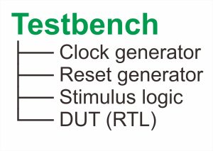
Figure 2. Illustration of a testbench
8. Why is the Testbench Not Synthesized?
Because the testbench uses the features:
- Time delay.
- Infinite loop.
- File I/O.
- Randomization
The above testbench features cannot be realized in hardware, so this is the reason why the testbench cannot be synthesized.
9. Common Mistakes of Digital System Designers
- Didn’t create a testbench.
- Assuming the RTL design is correct without simulation.
- Do not use reset.
- Didn’t test all scenarios.
Digital circuit design simulation using a testbench prevents all of these common possible errors.
10. Summary Explanation of Testbench
- Simulation is the process of virtually executing a digital/RTL design.
- Testbench is a simulation driver.
- RTL cannot be tested without a testbench.
- Simulation + testbench is the foundation of digital design.
- The larger the digital system or circuit design, the more important the testbench.
By understanding the relationship between simulation and testbench, a novice engineer can not only “write HDL code”, but also understand the behavior of digital circuit design systematically and professionally.
11. Example of Testbench Program Code
11.1 VHDL Program Code – Digital System Design & Testbench
The following is an example of a VHDL code pair for designing a digital “4-bit up-counter” circuit and its testbench.
A 4-bit up-counter is a sequential digital circuit that:
- Increments its value on every clock cycle.
- Counts from 0000 (0) to 1111 (15).
- Then wraps back to 0000 (overflow).
- Operates synchronously with a clock signal.
Program 1: VHDL program code for digital circuit design (counter.vhd)
|
1 2 3 4 5 6 7 8 9 10 11 12 13 14 15 16 17 18 19 20 21 22 23 24 25 26 27 28 |
library IEEE; use IEEE.STD_LOGIC_1164.ALL; use IEEE.NUMERIC_STD.ALL; entity up_counter_4bit is Port ( clk : in STD_LOGIC; rst : in STD_LOGIC; count : out STD_LOGIC_VECTOR (3 downto 0) ); end up_counter_4bit; architecture Behavioral of up_counter_4bit is signal counter_reg : UNSIGNED(3 downto 0) := (others => '0'); begin process(clk, rst) begin if rst = '1' then counter_reg <= (others => '0'); -- Reset to 0 elsif rising_edge(clk) then counter_reg <= counter_reg + 1; -- Increment end if; end process; count <= STD_LOGIC_VECTOR(counter_reg); // Output conversion end Behavioral; |
Explanation:
Explanation for the VHDL code (Program 1):
A. Used VHDL Libraries
|
1 2 3 |
library IEEE; use IEEE.STD_LOGIC_1164.ALL; use IEEE.NUMERIC_STD.ALL; |
Enables arithmetic operations (+, -, *, /) required because STD_LOGIC_VECTOR cannot be directly incremented.
B. Entity (Interface)
|
1 2 3 4 5 6 7 |
entity up_counter_4bit is Port ( clk : in STD_LOGIC; rst : in STD_LOGIC; count : out STD_LOGIC_VECTOR (3 downto 0) ); end up_counter_4bit; |
Defines inputs and outputs:
- clk = Clock signal.
- rst = Reset signal (active HIGH).
- count = 4-bit output
C. Define Internal Signal
|
1 |
signal counter_reg : UNSIGNED(3 downto 0) := (others => '0'); |
Uses UNSIGNED so arithmetic (+1) is valid. 4 bits range from 0 to 15.
D. Process Block (Core Logic)
D.1 Process Block 1: Reset Condition
|
1 2 |
if rst = '1' then counter_reg <= (others => '0'); |
- Asynchronous reset.
- Immediately sets counter to 0
D.2 Process Block 2: Clock Condition
|
1 2 |
elsif rising_edge(clk) then counter_reg <= counter_reg + 1; |
On every rising edge, the counter increments by 1.
Why rising_edge(clk)?
Because to ensures this design is a synchronous design.
E. Output Conversion
|
1 |
count <= STD_LOGIC_VECTOR(counter_reg); |
Converts UNSIGNED signal data type (counter_reg) to STD_LOGIC_VECTOR for the output.
Why UNSIGNED?
UNSIGNED data type allows an arithmetic operation, but STD_LOGIC_VECTOR data type alone cannot be incremented. So, the strategy for the process is use UNSIGNED on the arithmetic operation process, then convert it to STD_LOGIC_VECTOR data type once the process done.
Program 2: VHDL program code testbench for digital circuit design (tb_counter.vhd)
|
1 2 3 4 5 6 7 8 9 10 11 12 13 14 15 16 17 18 19 20 21 22 23 24 25 26 27 28 29 30 31 32 33 34 35 36 37 38 39 40 41 42 43 44 45 46 47 48 49 50 51 52 53 54 55 56 57 58 59 60 61 62 63 |
library IEEE; use IEEE.STD_LOGIC_1164.ALL; entity tb_up_counter_4bit is end tb_up_counter_4bit; architecture Behavioural of tb_up_counter_4bit is component up_counter_4bit Port ( clk : in STD_LOGIC; rst : in STD_LOGIC; count : out STD_LOGIC_VECTOR (3 downto 0) ); end component; signal clk : STD_LOGIC := '0'; signal rst : STD_LOGIC := '0'; signal count : STD_LOGIC_VECTOR (3 downto 0); begin -- Instantiate DUT uut: up_counter_4bit port map ( clk => clk, rst => rst, count => count ); -- Clock generation (10 ns period) clk_process : process begin while true loop clk <= '0'; wait for 5 ns; clk <= '1'; wait for 5 ns; end loop; end process; -- Stimulus process stim_proc: process begin -- Step 1: Apply reset rst <= '1'; wait for 20 ns; -- Step 2: Release reset rst <= '0'; -- Step 3: Run the counter wait for 200 ns; -- Step 4: Apply reset again rst <= '1'; wait for 20 ns; rst <= '0'; wait; end process; end Behavioural; |
Explanation:
Explanation for the VHDL testbench code (Program 2):
A. Used Libraries
|
1 2 |
library IEEE; use IEEE.STD_LOGIC_1164.ALL; |
Standard VHDL libraries should be declared as the same practice on the main VHDL code (Program 1) for the counter design.
B. Entity Declaration
|
1 2 |
entity tb_up_counter_4bit is end tb_up_counter_4bit; |
For the entity, we just need to type the entity block with no need to declare the I/O port lists as the same practice on the main VHDL code (Program 1).
C. Behavioural Architecture
|
1 |
tb_up_counter_4bit |
The architecture name of the VHDL testbench design is “tb_up_counter_4bit”
C.1 Behavioural Architecture 1: Counter Component
|
1 2 3 4 5 6 7 |
component up_counter_4bit Port ( clk : in STD_LOGIC; rst : in STD_LOGIC; count : out STD_LOGIC_VECTOR (3 downto 0) ); end component; |
In the behavioural architecture block, we need to declare the I/O port lists same with the I/O port lists that declared on the main VHDL code (Program 1).
C.2 Behavioral Architecture 2: Testbench Signal Initialization
|
1 2 3 |
signal clk : STD_LOGIC := '0'; signal rst : STD_LOGIC := '0'; signal count : STD_LOGIC_VECTOR (3 downto 0); |
At the testbench signal, we need to define the initial values for each of it.
C.3 Behavioral Architecture 3: DUT Instantiation
|
1 2 3 4 5 6 7 |
-- Instantiate DUT uut: up_counter_4bit port map ( clk => clk, rst => rst, count => count ); |
DUT instantiation will connect all the declared I/O port lists in the main VHDL code (Program 1) with the testbench signal that declared in the VHDL testbench code. Make sure all of the ports connect to the correct pairs, port clk with port clk, port rst with port rst, and port output count with port count.
C.4 Behavioral Architecture 4: Clock Generator
|
1 2 3 4 5 6 7 8 9 10 |
-- Clock generation (10 ns period) clk_process : process begin while true loop clk <= '0'; wait for 5 ns; clk <= '1'; wait for 5 ns; end loop; end process; |
This design use clock with 10 ns period and 100 MHz frequency.
C.5 Behavioral Architecture 5: Stimulus Process
|
1 2 3 4 5 6 7 8 9 10 11 12 13 14 15 16 17 18 19 20 |
-- Stimulus process stim_proc: process begin -- Step 1: Apply reset rst <= '1'; wait for 20 ns; -- Step 2: Release reset rst <= '0'; -- Step 3: Run the counter wait for 200 ns; -- Step 4: Apply reset again rst <= '1'; wait for 20 ns; rst <= '0'; wait; end process; |
The stimulus for the input behaviour triggered by followed the simulation steps below:
Step 1: Applying reset (rst <= 1, then wait for 20 ns).
Step 2: Release reset (rst <= 0).
Step 3: Run the counter (By wait for 200 ns).
Step 4: Apply reset again (rst <=1, wait for 20 ns, rst <= 0).
C.6 Simulation Output
In waveform viewer, count will increase every clock cycle and automatically wraps to 0000 after 15 times counting.
11.2 Verilog Program Code – Digital System Design & Testbench
The following is an example of a Verilog code pair for designing a digital “counter” circuit and its testbench. In this example, we will create 4-bit up-Counter design.
This counter:
- Counts from 0 to 15 (0000 to 1111).
- Has clock, reset, and enable.
- Synchronous design.
Program 3: Verilog program code for digital circuit design (counter.v)
|
1 2 3 4 5 6 7 8 9 10 11 12 13 14 15 |
module counter_4bit ( input wire clk, input wire rst, // synchronous reset input wire en, // enable output reg [3:0] count ); always @(posedge clk) begin if (rst) count <= 4'b0000; else if (en) count <= count + 1; end endmodule |
Explanation for the Verilog code (Program 3):
A. Module Name
|
1 2 3 4 5 6 |
module counter_4bit ( input wire clk, input wire rst, input wire en, output reg [3:0] count ); |
The meaning of this block code is:
module counter_4bit, this is the name of a module. The module declares all of the I/O hardware.
- clk = Clock signal (controls timing)
- rst = Reset signal
- en = Enable signal (turn counter ON/OFF)
- count = 4-bit output (values 0–15)
We use “output reg”, because “count” is updated inside an always block (sequential logic).
B. Sequential Logic with “always” keyword
|
1 |
always @(posedge clk) |
This is the core of the counter. It is a sequential logic.
The meaning of this block code is:
- This block runs every rising edge of the clock.
- This models flip-flops (registers) in real hardware.
- Think of it as, “Update the counter only when the clock ticks”
C. Reset (rst) condition check (If rst = 1)
|
1 2 |
if (rst) count <= 4'b0000; |
Meaning, If the reset = 1, then the counter becomes 0. Happens synchronously (only at clock edge).
Why synchronous reset?
- Safer for FPGA timing.
- Avoids glitches.
D. Reset (rst) condition check (If rst = 0)
|
1 2 |
else if (en) count <= count + 1; |
The meaning of this block code is:
If the reset = 0, enable the logic.
If enable = 1, increment the counter by 1 value. But, If enable = 0, do nothing (hold value).
This code will create a register with enable control. All registers update at the same time (parallel hardware).
On the “count” expression:
|
1 |
count <= count + 1; |
Why NOT use “=” operator?
Operator “<=” is non-blocking assignment (used for sequential logic).
Operator “=” is blocking assignment (used for combinational logic).
E. Summary of the Counter Behaviour
- When rst = 1, then result is count = 0
- When en = 1, then result is count increments (count + 1)
- When en = 0, then result is count holds
- When count = 15, then result will wrap back to 0
Program 4: Verilog program code testbench for digital circuit design (tb_counter.v)
This testbench will generates clock signal, applies reset, toggles enable, and observes output.
|
1 2 3 4 5 6 7 8 9 10 11 12 13 14 15 16 17 18 19 20 21 22 23 24 25 26 27 28 29 30 31 32 33 34 35 36 37 38 39 40 41 42 43 44 45 46 47 48 49 50 51 52 53 54 55 56 57 58 |
`timescale 1ns/1ps module tb_counter_4bit; reg clk; reg rst; reg en; wire [3:0] count; // Instantiate DUT (Device Under Test) counter_4bit uut ( .clk(clk), .rst(rst), .en(en), .count(count) ); // Clock generation (10ns for full period) always #5 clk = ~clk; // Step 1: Stimulus/Initialize signals initial begin clk = 0; rst = 1; en = 0; // Step 2: Apply reset #10; rst = 0; // Step 3: Enable counting #10; en = 1; // Step 4: Run the counter #100; // Step 5: Disable counting en = 0; #20; // Step 6: Enable again en = 1; #50; // Step 7: End simulation $finish; end // Step 8: Monitor values (Observes output) initial begin $monitor("Time=%0t | rst=%b en=%b count=%d", $time, rst, en, count); end endmodule |
Explanation for the Verilog testbench code (Program 4):
A testbench is NOT hardware. It is used only for simulation.
A. Testbench module
|
1 |
module tb_counter_4bit; |
No inputs/outputs needed at the testbench module name. It drives and observes the DUT (Design Under Test).
B. Signal declaration
|
1 2 3 4 |
reg clk; reg rst; reg en; wire [3:0] count; |
“reg” used to drive inputs (clk, rst, and en).
“wire” used to observe outputs.
C. DUT Instantiation
|
1 2 3 4 5 6 |
counter_4bit uut ( .clk(clk), .rst(rst), .en(en), .count(count) ); |
DUT instantiation make the testbench signals and counter inputs/outputs connected.
D. Clock Generation
|
1 |
always #5 clk = ~clk; |
Meaning, flip clock every 5 ns. For full period, the delay is 10 ns. This will simulate a real clock signal.
E. Simulation Steps
E.1 Simulation Step 1: Stimulus (Input Control)
|
1 2 3 4 5 |
// Initialize signals (Stimulus) initial begin clk = 0; rst = 1; en = 0; |
Define initial value for every testbench input signal.
E.2 Simulation Step 2: Apply Reset
|
1 2 |
#10; rst = 0; |
Hold the reset for 10 ns, then release (rst = 0).
E.3 Simulation Step 3: Start Counting
|
1 2 |
#10; en = 1; |
Enable counter (en = 1).
E.4 Simulation Step 4: Run the Counter
|
1 |
#100; |
Counter runs for 100 ns.
E.5 Simulation Step 5: Stop Counting
|
1 |
en = 0; |
Counter freezes.
E.6 Simulation Step 6: Enable Counter Again
|
1 2 |
#20; en = 1; |
Enable counter (en = 1) again.
E.7 Simulation Step 7: End Simulation
|
1 2 |
#50; $finish; |
E.8 Simulation Step 8: Observes Output
|
1 |
$monitor("Time=%0t | rst=%b en=%b count=%d", $time, rst, en, count); |
Meaning, prints values whenever something changes.
E.9 Example output of the simulation:
|
1 2 |
Time=20 | rst=0 en=1 count=1 Time=30 | rst=0 en=1 count=2 |
11.3 SystemVerilog Program Code – Digital System Design & Testbench
The following is an example of a SystemVerilog code pair for designing a digital “counter” circuit and its testbench. In this example, We will create 4-bit up-Counter design.
This counter design:
- Counts from 0 to 15 (0000 to 1111).
- Has clock, reset (synchronous), and enable signal.
- Synchronous design.
Program 5: SystemVerilog program code for digital circuit design (counter.sv)
|
1 2 3 4 5 6 7 8 9 10 11 12 13 14 15 16 |
module up_counter_4bit ( input logic clk, // Clock signal input logic reset, // Synchronous reset input logic enable, // Enable counting output logic [3:0] count // 4-bit output ); // Sequential logic: triggered on rising edge of clock always_ff @(posedge clk) begin if (reset) count <= 4'b0000; // Reset counter to 0 else if (enable) count <= count + 1; // Increment counter end endmodule |
Explanation for the SystemVerilog testbench code (Program 5):
A. Module Interface
|
1 2 3 4 5 6 |
module up_counter_4bit ( input logic clk, // Clock signal input logic reset, // Synchronous reset input logic enable, // Enable counting output logic [3:0] count // 4-bit output ); |
- Clk = Drives the counter (synchronous design)
- Reset = Clears counter to 0
- Enable = Controls whether counting happens
- Count = 4-bit output (range: 0–15)
B. Sequential Logic
|
1 |
always_ff @(posedge clk) |
- always_ff statement is SystemVerilog construct for flip-flop-based logic.
- Triggered on rising edge of clock (clk)
C. Reset Behaviour
|
1 2 |
if (reset) count <= 4'b0000; // Reset counter to 0 |
- Synchronous reset.
- Reset only happens at clock edge.
- Ensures stable hardware behavior.
D. Counting Logic
|
1 2 |
else if (enable) count <= count + 1; // Increment counter |
- Counter increments only when enable = 1
- If enable = 0, value is held (no change)
Program 6: SystemVerilog program code testbench for digital circuit design (tb_counter.sv)
|
1 2 3 4 5 6 7 8 9 10 11 12 13 14 15 16 17 18 19 20 21 22 23 24 25 26 27 28 29 30 31 32 33 34 35 36 37 38 39 40 41 42 43 44 45 46 47 48 49 50 51 52 53 54 55 56 57 58 59 60 61 62 63 64 65 66 |
// Timescale `timescale 1ns/1ps module tb_up_counter_4bit; // Step 1: Testbench signals declaration logic clk; logic reset; logic enable; logic [3:0] count; // Step 2: Instantiate the DUT (Device Under Test) up_counter_4bit uut ( .clk(clk), .reset(reset), .enable(enable), .count(count) ); // Step 3: Clock generation: 10 ns period always #5 clk = ~clk; // Test procedure initial begin // Step 4: Initialize signals clk = 0; reset = 1; enable = 0; // Step 5: Apply reset #10; reset = 0; // Step 6: Enable counting enable = 1; // Step 7: Run the counter for some cycles #100; // Step 8: Disable counting enable = 0; #20; // Step 9: Re-enable counting enable = 1; #50; // Step 10: Apply reset again reset = 1; #10; reset = 0; #50; // Step 11: End simulation $finish; end // Monitor output initial begin $monitor("Time=%0t | reset=%b enable=%b count=%b", $time, reset, enable, count); end endmodule |
Explanation for the SystemVerilog testbench code (Program 6):
A. Timescale declaration
|
1 |
`timescale 1ns/1ps |
Timescale is a compiler directive in Verilog/SystemVerilog that defines how time is interpreted in simulation. It does not affect hardware, only simulation behavior.
1ns (time unit) : Base unit of time used in delays
1ps (time precision) : Smallest resolution for rounding time
B. Simulation Steps
B.1 Simulation Step 1: Testbench Signal Declaration
|
1 2 3 4 5 |
// Step 1: Testbench signals declaration logic clk; logic reset; logic enable; logic [3:0] count; |
Declare all signal based on the counter design (RTL), Program 5.
B.2 Simulation Step 2: DUT instantiation
|
1 2 3 4 5 6 7 |
// Step 2: Instantiate the DUT (Device Under Test) up_counter_4bit uut ( .clk(clk), .reset(reset), .enable(enable), .count(count) ); |
Connects all testbench signals to all the design signal. Make sure, that we connect all the signal correctly. clk signal with clk, reset signal with reset, signal enable with enable, and signal output count with count.
B.3 Simulation Step 3: Clock Generation
|
1 2 |
// Step 3: Clock generation: 10 ns period always #5 clk = ~clk; |
Create a clock with 10 ns period and 100 MHz frequency.
B.4 Simulation Step 4: Signal Initialization
|
1 2 3 4 |
// Step 4: Initialize signals clk = 0; reset = 1; enable = 0; |
Apply initial value for the input signal (clk, reset, and enable). Reset signal state is active (reset = 1).
B.5 Simulation Step 5: Apply Reset
|
1 2 3 |
// Step 5: Apply reset #10; reset = 0; |
Release reset after 10 ns (reset = 0).
B.6 Simulation Step 6: Enable Counter
|
1 2 |
// Step 6: Enable counting enable = 1; |
Start counting, set the enable signal to one (enable = 1).
B.7 Simulation Step 7: Run the Counter
|
1 2 |
// Step 7: Run the counter for some cycles #100; |
Run the counter for 10 clock cycles (Delays #100).
B.8 Simulation Step 8: Disable Counter
|
1 2 |
// Step 8: Disable counting enable = 0; |
Pause counting, reset the enable signal to zero (enable = 0).
B.9 Simulation Step 9: Re-enable Counter
|
1 2 |
// Step 9: Re-enable counting enable = 1; |
Resume counting by set the enable signal to one (enable = 1) again.
B.10 Simulation Step 10: Apply Reset Again
|
1 2 3 4 |
// Step 10: Apply reset again reset = 1; #10; reset = 0; |
Apply reset again during operation.
B.11 Simulation Step 11: End Simulation
|
1 2 |
// Step 11: End simulation $finish; |
End the simulation process with $finish statement.
C. Output Monitoring
|
1 2 3 4 |
// Monitor output initial begin $monitor("Time=%0t | reset=%b enable=%b count=%b", $time, reset, enable, count); |
- Prints signal values whenever they change.
- Helps debug waveform behaviours.
D. Expected Output Simulation Behaviour
When reset = 1, then count = 0
When enable = 1, then count increments
When enable = 0, then count holds value
When counter overflow, then wraps to 0