Friends of Robonesia, if you are asked, “What is the name of the electronic component that is the most important and has the biggest influence in the development of the world of modern electronics?”
Yes, you are right, the answer is “IC” or the abbreviation for Integrated Circuit.
We all know that almost all electronic devices we use, from smartphones and laptops to TVs and electric cars to smart home devices, use integrated circuits (ICs) to operate quickly, efficiently, and accurately. This article will provide a comprehensive and easy-to-understand explanation of ICs, covering their definition, materials used, how they work, their uses, and even their manufacturing technology.
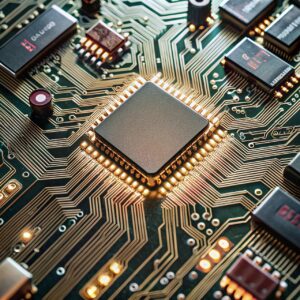
Gambar 1. Integrated circuits (IC)
Sumber: pixabay
1. What is an Integrated Circuit (IC)?
An Integrated Circuit (IC) is a miniature electronic component containing thousands to billions of transistors, resistors, capacitors, and diodes integrated into a single semiconductor chip, usually made of silicon. An IC acts as the brain or control center, enabling electronic devices to process signals, calculate data, store information, or control other devices quickly and efficiently.
Before the IC was invented in the late 1950s, electronic circuits were made from discrete components that were large, heavy, power-hungry, and prone to damage. The invention of the IC revolutionized technology by allowing circuits that were previously the size of a table to be reduced to just a few millimeters without losing functionality. The IC changed everything by providing:
- Smaller network size.
- Low power consumption.
- High performance.
- Lower production costs.
- Better reliability.
- This is why ICs have become a key component in the digital world revolution.
2. Why is IC so important?
The presence of IC is very important because it brings four major changes in the world of electronics technology:
2.1 Miniaturization of Electronic Devices
Currently, modern electronic devices, such as: smartphones, laptops, smartwatches, drones, and even electric cars can be made thin and light because the core components inside them use very small ICs.
2.2 Low Power Consumption
ICs use semiconductor materials with energy-saving characteristics, allowing devices such as laptops or cell phones to work longer on battery.
2.3 High Processing Speed
The transistors inside the IC can operate in nanoseconds. This allows modern computers to perform complex calculations, run AI applications, and even process 3D graphics quickly.
2.4 Lower Production Costs
Although IC fabrication technology is very expensive, mass production of ICs is much cheaper than electronic circuits with discrete components. This makes electronic devices affordable and can be produced in large quantities.
Undeniably, integrated circuits (ICs) are the foundation of all modern electronic devices. Without them, there would be no internet, computers, smartphones, AI, intelligent robots, or autonomous vehicles as we know them today. ICs are the backbone of the digital age and continue to evolve toward smaller, faster, and more efficient sizes.
3. IC Making Materials
ICs are made using semiconductor materials, mainly:
3.1 Silicon (Si)
The most common material because:
- Easy to get.
- Stable.
- Mature fabrication process.
- The cost is relatively cheap
3.2 Germanium (Ge)
Used in some high-speed applications, but not as popular as silicon.
3.3 Gallium Arsenide (GaAs)
Used in RF applications, satellite communications, radar, and high frequency devices.
3.4 Other advanced materials
Used for the latest generation of ICs:
- Silicon Carbide (SiC) for high power applications.
- Gallium Nitride (GaN) for power devices and 5G.
- Graphene (still under research) has the potential to bring ultra-fast computing.
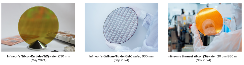
Figure 2. Infineon semiconductor wafer
Source: www.infineon.com
4. Types of ICs
ICs can be distinguished based on their function:
4.1 Digital ICs
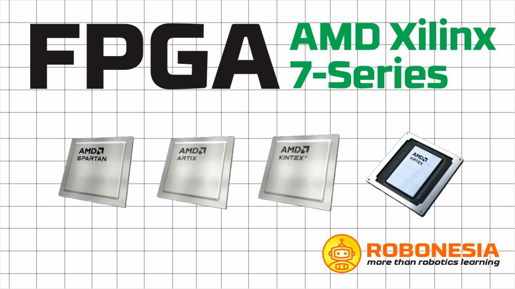
Digital ICs are ICs that process binary signals 0 and 1. Binary signals are also called digital signals. Examples of digital ICs include microprocessors, microcontrollers, memory (RAM, ROM), and FPGAs.
4.2 Analog ICs
Analog ICs are ICs that function to process analog signals (continuous signals). Examples of analog ICs are amplifiers, sensor interfaces, ADC/DAC.
4.3 Mixed-Signal ICs
Mixed-Signal ICs are ICs that process a combination of digital and analog signals in a single chip. Examples of mixed-signal ICs include communication ICs, audio codecs, power management ICs, and so on.
5. Functions and Uses of IC in Daily Life
ICs can be found in almost all modern technologies, such as:
5.1 Smartphones and Computers
- CPU
- GPU
- 5G Modem
- Camera sensor
5.2 Automotive
- ECU (Engine Control Unit).
- ABS system.
- Radar and LiDAR autonomous cars
5.3 Industry and Robotics
- Motor control.
- Automation system.
- Intelligent sensors and actuators
5.4 Consumer Electronics
- TV.
- Refrigerator.
- Smart AC.
- IoT devices
5.5 Medical and Health
- Ultrasound equipment.
- ECG Sensor.
- Wearable health tracker
6. How are ICs Made?
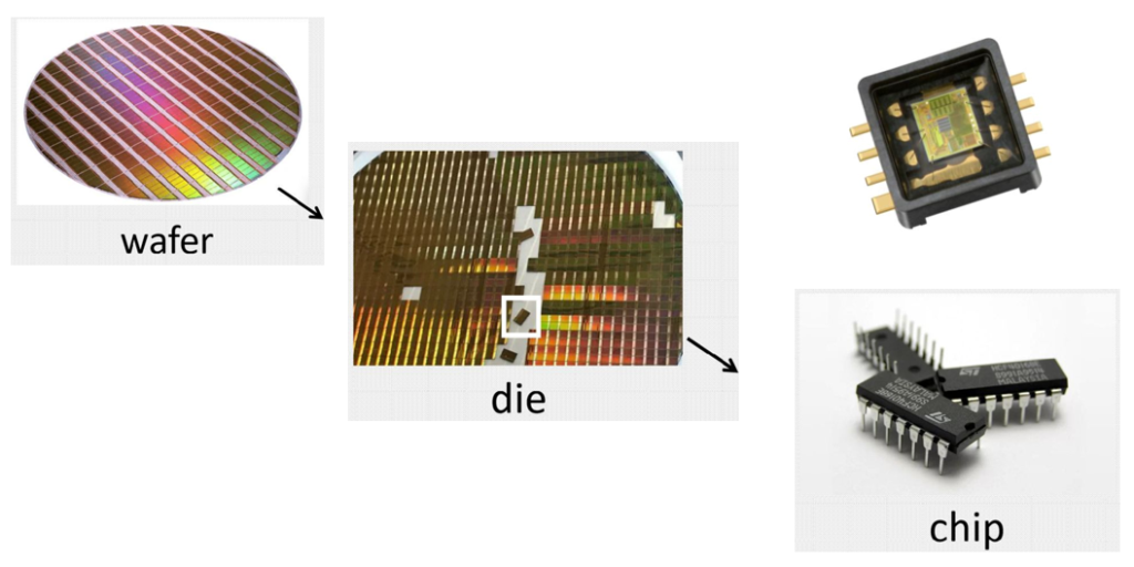
Figure 3. From semiconductor wafer to IC
Source: www.infineon.com
IC manufacturing is a complex process carried out in specialized facilities called semiconductor fabrication plants (fabs). The following are the main stages of the IC manufacturing process:
6.1 IC Design (Design Phase)
Includes:
- Architectural design.
- RTL design (with HDL such as VHDL/Verilog/SystemVerilog).
- Verification (UVM, simulation).
- Physical design (floor planning, placement-routing).
- Timing analysis.
- Tape-out
6.2 Wafer Fabrication
Using pure silicon in the form of discs.
6.3 Lithography
Transferring circuit patterns to the wafer surface using UV light.
6.4 Doping
Adding impurities to form a transistor (pn junction).
6.5 Etching
Scraping certain areas to form circuit paths.
6.6 Deposition
Adding a layer of metal, oxide, or other material.
6.7 Assembly
This process consists of the pre-assembly process (Waffer cutting) and the assembly process (Chip die bonding, wire bonding, molding, pad trimming, and pad forming).
6.8 Testing
Conducting tests on IC chips that have gone through the assembly process, namely electrical parameter tests and functional tests.
6.9 Packing
Packing the IC into a package (plastic tube or reel) before sending it to the customer.
All of the above processes require super-precision equipment, a dust-free room (clean room), and high-level manufacturing standards.
7. Development of IC Technology
IC technology is evolving rapidly, from micrometer to nanometer generations. For example: 90 nm, 45 nm, 14 nm, 7 nm, 5 nm, and 3 nm. The smaller the “process node,” the more transistors can be packed into a single chip, resulting in increased performance and greater power efficiency.
Latest technology:
- FinFET.
- GAAFET (Gate-All-Around FET).
- 3D IC (chip stacking).
- Chiplet architecture (used by AMD, Intel, Apple)
8. Advantages and Disadvantages of IC
8.1 Advantages:
- Very small size.
- Save power.
- High speed.
- Cheap in mass production.
- Makes electronic system performance more reliable.
8.2 Disadvantages:
- Difficult to repair if damaged.
- Requires a very expensive fabrication process.
- Has a maximum heat limit.
9. Conclusion
Integrated circuits (ICs) are the most fundamental components in modern technology. Without ICs, there would be no computers, smartphones, the internet, artificial intelligence, intelligent robots, or even autonomous vehicles. Understanding IC fundamentals provides a crucial foundation for anyone interested in electronics, robotics, embedded systems, or modern chip design.