Hello Robonesians, after previously we have studied together the HDL hardware description programming language, namely VHDL , in this article and God willing, in the next few articles, we will invite all friends to learn the HDL programming language which is the successor to the VHDL programming language, namely the Verilog programming language.
1.1 What is Verilog ?
Verilog is the second most popular hardware description language (HDL) after VHDL. Like VHDL, Verilog can also be used to design digital electronic hardware systems. It was developed in the mid-1980s and later transferred to the IEEE (Institute of Electrical and Electronics Engineers). It is formally defined by IEEE Standard 1364. This standard was ratified in 1995 (referred to as Verilog-1995), revised in 2001 (referred to as Verilog-2001), and in 2005 (referred to as Verilog-2005). Many useful enhancements were added in the revised version.
In 1985, Automated Integrated Design Systems (renamed Gateway Design Automation in 1986) introduced a product called Verilog. This product was the first logic simulator to combine high-level programming language and gate-level simulation. Before Verilog, there were many gate-level simulators and some high-level programming language simulators, but there was no way to easily combine them. Around the same time, Gateway added the XL algorithm to its product, creating Verilog-XL. This addition of the algorithm is what made Verilog even more popular.
The XL algorithm accelerated gate simulation, making Verilog the fastest gate-level software simulator at the time. Even faster than some existing hardware accelerators. Several simulators use Verilog today.
1.2 Digital System Design Creation Flow
The general flow for designing a digital electronic circuit or system can be explained in Figure 1 below.
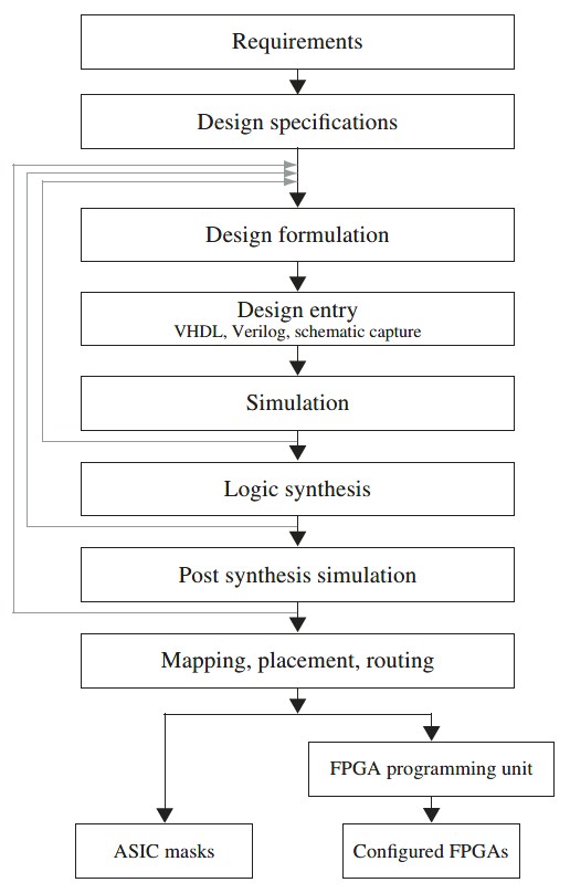
Figure 1. Digital system design creation flow
Source: Digital Systems Design Using Verilog (Charles Roth, Lizy K. John, Byeong Kil Lee) – Page 59
Figure 1 illustrates the steps or flow in creating a modern digital system design and below is a brief explanation of each step.
Step 1: Description of system requirements (Requirements)
The first step in the design flow is to describe the system requirements to be built based on consumer or market demand.
Step 2: Design specification
The output of step-1 is the design specification. The design specification of a digital system or circuit can be a description of the function (use/application) of the digital system to be built, the determination of what digital components will be used (registers, multiplexers, counters, logic gates, flip-flops, and so on), the number of input/output lines required, the type of interface (UART, I2C, SPI, and so on) used, and so on.
After the design specifications are described, the digital system circuit design flow can continue to the design formulation step (Step 3).
Step 3: Design formulation
Design formulation of digital system circuits is carried out at the concept level, both at the block diagram level and at the algorithm level.
Step 4: Design Entry
Design entry for digital system circuits can be done in two ways: Method 1: Design a digital system circuit using graphical methods using CAD (Computer-Aided Design) software, such as OrCAD, Altium Designer, Allegro, or others. Method 2: Design a digital system circuit using text or HDL programming languages. Three popular HDL programming languages today are VHDL, Verilog, and SystemVerilog. This second method is what we will learn in articles related to the topic of digital system design on the robonesia website.
Step 5: Pre-Synthesis Simulation
After the design entry stage, the next stage is a simulation of the digital system circuit design before the design is synthesized (Pre-synthesis simulation). This pre-synthesis simulation is necessary to ensure that the design functions (Functional simulation) correctly according to the concepts and specifications created in the previous stage. Pre-synthesis simulation is performed on a high-level behavioral model of the digital system design. Pre-synthesis simulation will reveal problems or errors in the design early before the digital system design is synthesized. If problems or errors are found during the pre-synthesis simulation stage, the digital system designer can examine and correct the design errors that occur so that they meet the expected requirements and specifications.
Step 6: Logic synthesis
After the design functionality has been verified through pre-synthesis simulation, the next step is to synthesize the digital system or circuit design. Synthesis involves converting or compiling a high-level abstract description of the design into actual components at the gate and flip-flop level. The output of the synthesis process is a gate list and a netlist, which define the interconnections between the digital system components in the design.
Step 7: Post-Synthesis Simulation
After the logic synthesis stage, the next stage is the simulation of the digital system circuit design after the design is synthesized (Post-synthesis simulation). In the previous pre-synthesis simulation stage (Step 5), the simulation was carried out on a high-level digital system design behavioral model without paying attention to the implementation specifications of the target programmable device hardware components used in the design (behavioral model). Meanwhile, the post-synthesis simulation was carried out on a digital system design structural model by paying attention to the implementation specifications of the target hardware components or physical devices used in the design. The structural model of a design can be considered as a textual description (HDL program) that connects logic gates, flip-flops, counters, registers, and other modules.
Post-synthesis simulations are necessary to ensure and increase the level of confidence of digital system designers, that their digital system designs are suitable for production. However, if errors occur during the post-synthesis simulation stage, the designer must re-examine and modify the design to meet the expected requirements and specifications. This is normal or common, because to achieve proper design implementation (without errors), the process of verification through repeated (iterative) simulation is essential.
Step 8: Mapping, Placement, and Route (Implementation)
After the post-synthesis simulation phase, the next stage is mapping, placing, and routing the components within the digital system design created on the target programmable device (physical device) hardware. This stage is also known as the implementation stage.
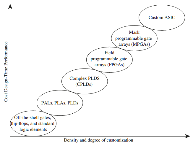
Figure 2. Programmable device technology
Source: Digital Systems Design Using Verilog (Charles Roth, Lizy K. John, Byeong Kil Lee) – Page 61
The target programmable device technology used for implementing digital system or circuit designs can be PLA, PAL, PLD, CPLD, FPGA, MPGA, or ASIC. Figure 2 provides information related to the comparison of the density level (Density), the number of gates that can be implemented, the level of customization (Degree of customization), design cost (Cost design), and time-performance (Time-performance) for each programmable device technology.
At the lowest level of sophistication and density are the old-fashioned printed circuit boards (PCBs) with logic gates, flip-flops, and standard logic building blocks. Slightly higher in density are programmable logic arrays (PLAs), programmable array logic (PALs), and simple programmable logic devices (SPLDs). PLDs with even higher density and gate counts are called complex programmable logic devices (CPLDs). Additionally, there are the popular field programmable gate arrays (FPGAs) and mask programmable gate arrays (MPGAs). The highest level of density and performance is the fully custom application-specific integrated circuit (ASIC).
The initial steps in the digital system design flow are largely the same for all of these target technologies (Figure 2). In the final stages of the design flow, different operations are performed depending on the target technology used.
The most common target technologies used today are FPGAs and ASICs. In step 8, the design is mapped to a specific target technology and placed within the target technology (e.g., using an ASIC or FPGA). The path taken by the connections between components is determined during the routing process.
If an ASIC is being designed, the routed design is used to generate a Photomask that will be used in the integrated circuit (IC) manufacturing process.
If the design is to be implemented on an FPGA, it is translated into a format that specifies what to do at various programmable points within the FPGA. In modern FPGAs, programming simply involves writing a sequence of 0s and 1s into a “programmable cell (CLB)” within the FPGA, and no special programming unit other than a personal computer (PC) is required to program an FPGA.
1.3 Electronics Design Automation (EDA) Tools
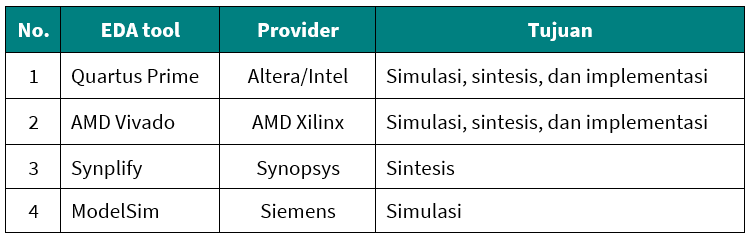
In the semiconductor industry, there are several EDA (Electronic Design Automation) software available for the purposes of simulating, synthesizing, and implementing electronic circuits using Verilog code, including the following:
Table 1. EDA tool references
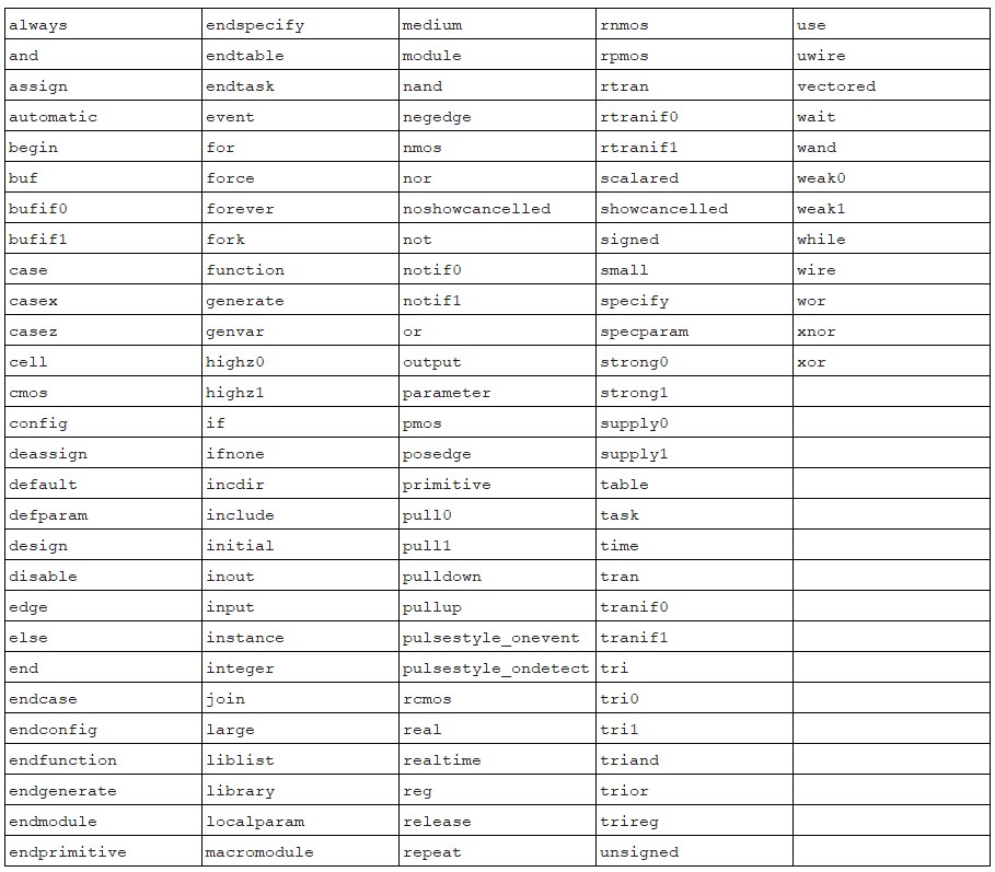
1.4 Keywords Used by Verilog (Reserved Keywords)
Like other programming languages, Verilog uses keywords. Digital system designers using Verilog must be aware of reserved keywords in Verilog so they don’t use them when creating Verilog program statements. Below is a table of keywords used by Verilog.
Table 2. List of Verilog keywords (Verilog IEEE Standard 2005)
Source: Digital Systems Design Using Verilog – Charles Roth, Lizy K. John, Byeong Kil Lee – Page 562-563